|
Retrocomputing is always a lot of fun. Machines which you can fully
understand and fully control are exceedingly rare in these days of
complex computing. When you sat down to a machine like a Commodore 64
or an Apple II, you were certainly the one in charge.
Some machines take this a little farther. These machines, which
we colloquially call “blinking light machines” let you peer into their
operations a little more deeply. For example, I have an Altair 8800
clone as well as the PiDP-8 and PiDP-11 kits. All of these machines
have lights which allow you to see the memory and data buses of the
processor along with varying amounts of information about their CPU’s
internal state. Even better, these machines have a bank of switches
which allow the programmer to directly put a binary machine code
program in memory. These machines operate without even the slightest
pretense of abstraction, and they also make delightful blinking
patterns.
The thing of it is, all of my blinking light machines up until now
have been illusions. My Altair is based on a microcontroller which
emulates a fully loaded machine (about $16,000 worth of hardware in
1975 dollars, or $64,000 when adjusted for inflation!) The PiDP kits
are based on simh running on a raspberry pi. These machines all
provide a good emulation of the original experience, but the hardware
interactions are still an illusion. That is why I was so excited to
learn about another blinking light computer kit, Lee Hart’s
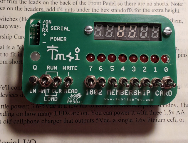
1802 Membership Card.
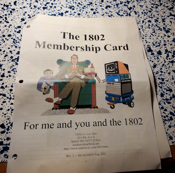
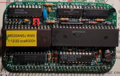
This machine is a reproduction of the COSMAC ELF machine that was
introduced as a DIY computer in a 1976 issue of Popular Electronics.
I had been vaguely aware of the ELF, but never really gave it much
thought. It was a sort of footnote in my knowledge of microcomputing
history. So I read a little bit of the 1976 article and I read the
membership card website and came to the conclusion that I just had to
build this little blinking light machine. Even better, this is no
simulation, it is a real 1802 processor surrounded by period correct
parts!
I put in an order via the sunrise-ev
website. Like many hobby kits, it is sold via simple PayPal invoicing.
As I was ordering two things, the full membership card kit and a ROM
chip, I used an email-based order form so that it would have correct
shipping. I received a PayPal invoice within 24 hours of emailing Mr.
Hart, and then I received the kit approximately seven days later.
After I sent in the payment, I printed out the membership card manual
and spent some time studying up on the construction process as well as
the front panel operations.
When the kit arrived, I was pleasantly surprised to see that it
included a color printed manual. I knew that it included a manual,
I was just not expecting such a nicely printed copy! Also, note that
it arrived with 3 holes already punched for easy binder installation.
It also reads like a hobbyist manual from the era, so it is a real
delight to work with.
The manual explains that “this is an adventure, by cracky!” a clear
callback to the Captain Cozmo’s Whizbang book which is linked from the
manual’s pdf. The membership card is our gateway into the world of
microcomputing, and the first step of the journey is to pass an
aptitude test. We are to unpack and catalog each of the parts, and
prepare for assembly. The manual gives us a handy form to do this,
checking off each component as we go. The kit was shipped with its
components inside of the Altoids tin which will ultimately serve as
the machine’s case. There are two small baggies inside which were
labeled “CPU” and “Front Panel.” I began construction last Thursday
evening and decided I would build the CPU board on Thursday and the
front panel on Friday.
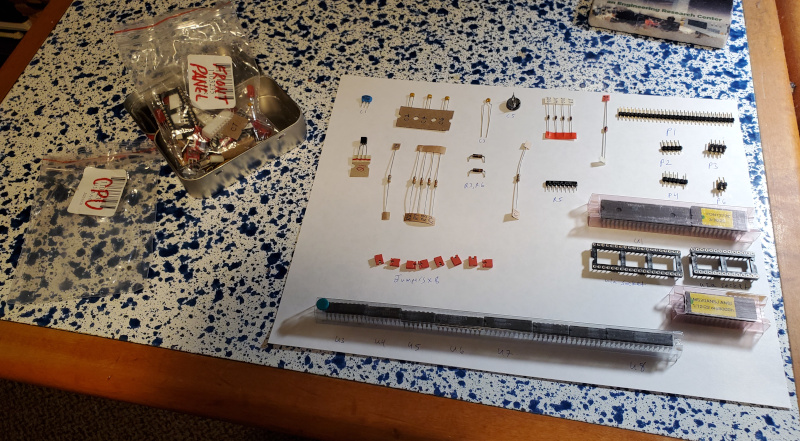
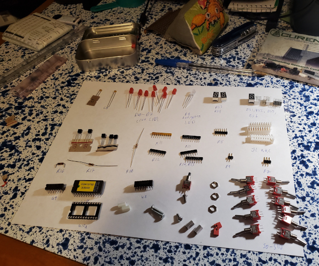
I believe I passed the aptitude test. As I took inventory of the CPU
parts, I did what I typically do with a kit. I placed the parts on
a piece of paper and labeled them. Apparently, Lee thinks
the same way. (I feel that after the informal tone of the manual,
I can call him by his first name. He can certainly call me “Bob”
should we ever meet.) Also, he has thoroughly designed his board and
labeled every component with a letter and a number. A nice
professional touch that not all kits follow! Even better, the
components that were on tape strips arrived already labeled. This last
bit is why I think Lee and I are on the same wavelength. I would have
done this as I found each part. This makes the kit somewhat friendly
to beginning level builders, though I would not recommend the
membership card to someone new to soldering!
I fired up my trusty low-cost digitally controlled soldering iron and
dialed it into 290 degrees Celsius. I am using 63/37 solder, with all
of its luxurious lead. Lead-free solder is definitely the wrong
choice for this board as the pads are close and small, and so reliable flow is
a must! Those in the know will note that I set my iron to about 100
degrees above 63/37’s typical melting point. I do this because this is
a very fine tipped soldering iron and if I set it right at the melting
point heat transmission takes a bit too long. I prefer to flow quickly
and reliably, and this is about the point where I can do that with
this tip.
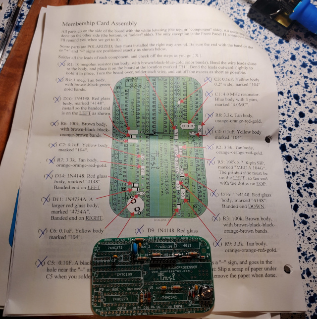
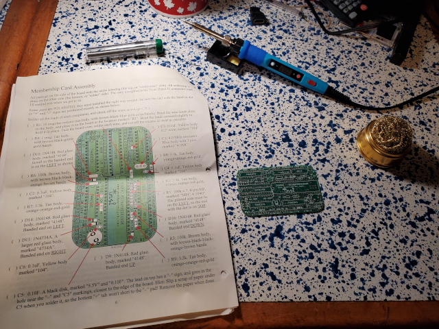
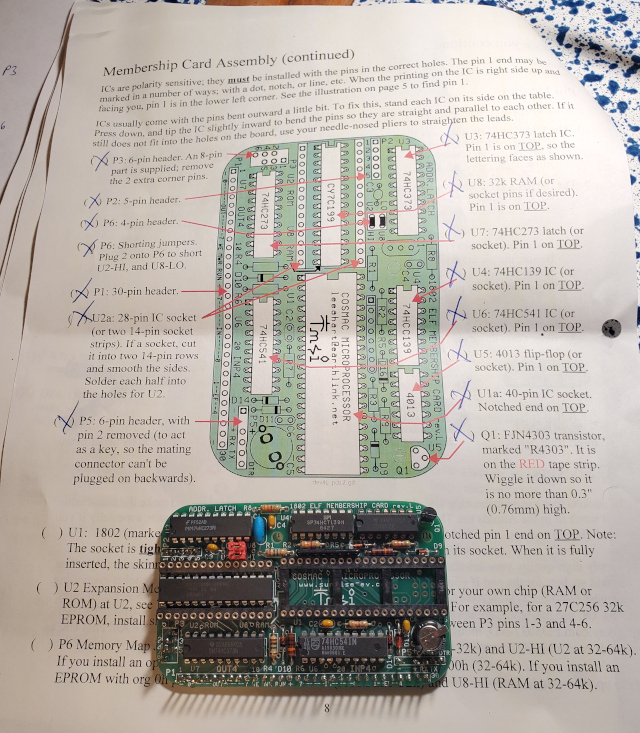
Did I mention before that this manual is a pure delight? Well, it
bares repeating! I love that on a single page we get a check list that
also shows us where to put everything. Most of the positions on the
board are screen printed, but sometimes close components make
identifying the correct holes difficult. Having this
picture clears up the confusion. Working slowly and methodically,
I had no trouble finding the correct position of each component.
I decided to build the board up according to the hight of the
components. I did the diodes (all denoted as D followed by a number),
then the resistors (R), and finally the capacitors and crystal (C).
I had trouble
finding the right bend spot for the leads on a couple of diodes, but
I generally found the hole spacing easy to work with and wound up with
a relatively neatly aligned board.
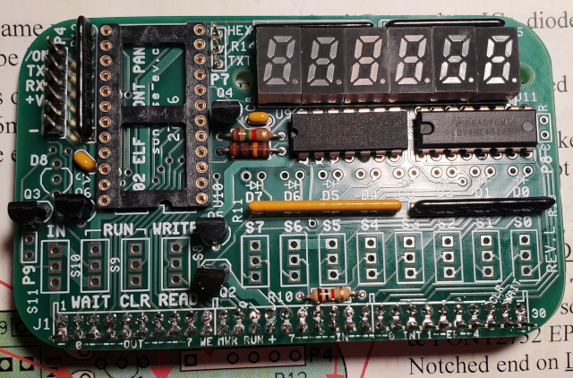
The construction of the CPU board is done in two main parts. The first
was to put all the discrete components in place. This is what was on
this page, and here is a closeup of the board after that page.
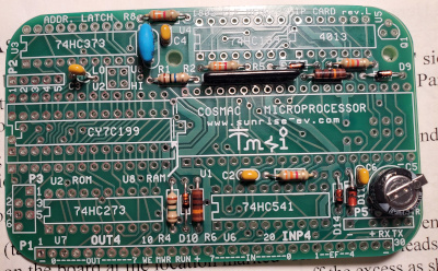
You can also see the fine work done in the PCB. It is well designed
and period correct. There is no fiddly surface mounting to be done. It
is all through hole components on a dual sided PCB. There is no reason
this board could not be built in the late 70s or early 80s.
One thing I dig about this design is the super capacitor in the
lower right hand side. This is used to drive the RAM after power is
removed, thus the membership card will retain its contents when it is
powered off. The CPU will lose state, but loaded programs will remain
for quite a while after power down. This was also sort of a feature of
the original ELF, with several hobbyist adding RAM backup batteries so
they did not have to re toggle their machine code all the time. This
is a really nice feature for microcomputers of the era.
 Ok, on to the second part of CPU construction! I elected to take care
of the sockets and headers first and then solder the ICs that are
directly attached to the board in place.
Ok, on to the second part of CPU construction! I elected to take care
of the sockets and headers first and then solder the ICs that are
directly attached to the board in place.
The headers are probably the most difficult part of everything. The
instructions outline an easy way and a hard way. The easy way is to
drop the pins in place and then solder them from the back of the card.
You should only do this if you are not building the front panel card
though! It mentions that you can do this unless you want to fit both
boards in the Altoids tin, but the headers and stand offs used to
assemble the two boards into one unit only have clearance enough for
the hard way. The hard way is to push the plastic strip down on the
pins and then install them from underneath. You solder them on to the
top of the board and then cut off the plastic strips and cut the pins
flush with the bottom of the board.
Because I am building both boards, I elected to do the hard way.
It was not all that difficult, but probably one of the harder parts of
the kit to construct.
Another thing that gave me a bit of trouble can be seen on the left of
the board. In order to save space, the optional ROM chip straddles
a rather narrow 32K RAM chip. In order to accomplish this, the
instructions have you cut apart the ROM’s socket. When I did this, and
smoothed out the contacts, it made the socket a little harder to keep
aligned while soldering. I held it in place with masking tape, but
it managed to travel a bit upwards which makes my ROM chip sit
a little too high, thus negating all my careful work with the header
pins! If I had it to do over, I would have first soldered the ROM
socket in place, and then clipped the plastic once it was on the
board. So if you build one, you should do that.
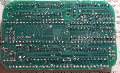
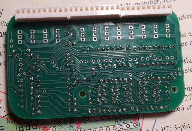
Here, you can see the back of the board after all of the soldering.
Note that this is close work. Be careful of dry joints and cold
joints! Desoldering on this would be a bit difficult, so take your
time and do things correctly the first time. Nevertheless, I found it
to be reasonably easy to work with. I had no burnt areas, though I do
have a bit of flux to clean up. Also, note that the bottom of the
board is where the headers are. They look rough, but remember they are
soldered on the component side of the board. They look rough because
I have been at them with a pair of side cutters! You can see the other
headers on the board have the same treatment.
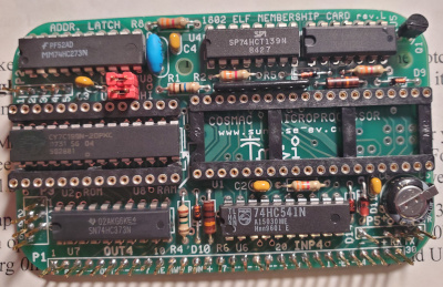
After a little bit of fiddling with the chips, I have them installed
in their sockets and the CPU board is complete! We see the ROM on the
left and the CPU is on the right. The RAM cannot be seen because it is
beneath the ROM chip.
A word of advice
on the socket front. If you work with ICs, an
IC
Pin Straightener too is a must-have.
ICs have pins bent out slightly when they ship, and these things will
move them into a right angle which are perfect for inserting through
holes and into sockets. Oh, and don’t get these from places like eBay
or Mouser. I’ve seen them go for $75.00. You can get them much more
cheaply. Don’t give more than $10.00 for a pin straightener!
So with the CPU board completed, I turned in for the night. Friday
I taught two of my favorite classes (a theory of computation course
and an operating system course) but I spent most of the day dreaming
of the things I would do with my 1802. After all, I have never
programmed an 1802 and I was excited to meet my new friend!
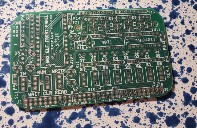
The front panel instructions were pretty much like the CPU
instructions. First, I inventoried the parts and then set to work. One
thing to notice about this board is the 7-segment display ports. The
original version of the kit had six displays which printed out ASCII
text. This revision only comes with two displays which automatically
renders the contents of the output port in hexadecimal on digits three
and four. There is a jumper which allows you to select which set of
characters will be generated by the ROM which drives the displays.
When I ordered the kit, I knew about this because I had read the
manual. I decided that I also wanted those additional displays so
I could play with the ASCII option. I have this vision of taking this
to my assembly and organization class next semester and toggling in
a “hello world” program which then displays on the front panel.
To pull this off, I double checked the schematics in the manual and
saw that these display units share a common conductor across the pins
and then are activated via latching the common ground. This meant that
if I simply purchased the additional components, I should be able to
have all six displays. So that is just what I did. These displays are
readily available at Mouser Electronics (
Part
Number 696-LDS-A3506RD.) I ordered four of these the same day I ordered
my 1802 membership card. They arrived the day before the kit, and so
I included them in my build.
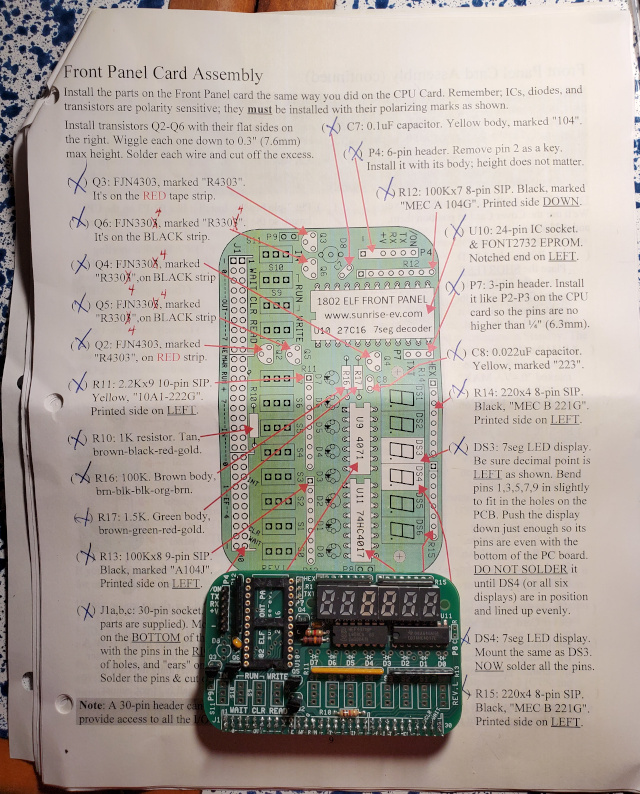
The first step in building the front panel is to put all of the
discrete components and sockets in place. Again, I worked my way up in
order of height. One of the trickiest parts of this section are the
displays. Rather than have the holes in a straight line, they are in
a sort of zig-zag pattern, probably due to sizing constraints. The
instructions tell you which pins to bend to get them through the
holes, and if you follow those it is reasonably easy. Also, I noticed
that there was a slight mismatch between the backgrounds of my
displays and the ones that came with the kit. So I put the two that
came with the kit in positions 3 and 4 (these are the digits you are
supposed to have), and then the other four surround them. You can see
that color difference in the photo, even though I did use the
specified part number. I suppose there is some variation between lots
or something.
In addition to the socket for the display driver, there is a line of
connectors on the bottom used to mate the front panel with the CPU
board. There is an optional row of headers that can be added at the
bottom, and I supplied the header strip for that from my own stock of
parts. For these and the jumper pins, I once again used the “hard
method” of assembly because they have to clear the back of the front
panel’s cover board. The pins on the left are mounted in the usual way
with the plastic strip on the component board. These are the serial
port and power connections, which need to be accessible when the cover
is on.
The ICs on this board serve to latch the display as well as provide
input from the switches. You can see the connection points for the
switches and push button on the board, and the next step is to add
those components in.
As I put this together, I renewed a bit confusion that I had about
what the front panel operations would be like for this system. With
only 8 lights, it must be the case that it visualizes the data bus.
This turned out to be incorrect. These lights are plugged into an
output port of the 1802. A cursory bit of reading in the information
from Popular Electronics seems to suggest that the 1802 provides some
front panel operations itself. I am not sure if this is the case but
I will investigate further later. I looked in the manual and realized
that there would be no visualization of the address bus, and that both
the switches and lights should be under fairly easy program control.
This is different from other blinking light systems I have used, so
I am intrigued!
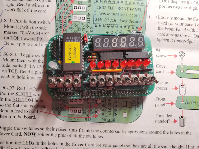
The front panel is finished by adding the lights and switches. The
front panel cover acts a sort of jig so you can align the switches and
lights and get everything at the right height. This made soldering the
switches and lights very easy. The instructions have you put the
halves together and then fasten them lightly with the screws beside
the display. I did this, but I neglected to put the spacers in place.
This meant my switches were fine but my lights were a little too short
as they were pushed into the board. When the cover is in place with
the spacers, they do not quite poke out, but they are plenty visible.
Oh well, these little variations are what make each membership card
special!
The final assembly step is to put the the two boards together. Here,
I discovered that my problem with the ROM IC meant that the two parts
won’t mount evenly. But with a little bit of light pressure on the
screws I was able to get them to go together a bit. I think I will
have to redo the ROM socket.
When I powered it on, it lit up! At first I was a bit disappointed.
After all, building a kit is fun but debugging a kit should always be
a part of the experience. I tried to insert some data into memory.
I reset the 1802, and I put the number zero in. I saw “00” on the hex
display, and no lights were on. In the next byte, I set my switches to
put in a one, and I saw “01” on the hex display and “00000001” on the
lights. So far so good! Then I put in two on the switches, and I saw
no lights and “00”. Uh oh….
A little more testing revealed that only the bit 0 switch appears to
be working on the data input. I can insert a 0, or I can insert
a 1.Those are my only two bytes. Oh joy! I get to debug things!
But that is where I will leave off for now. I put the kit together and
my evenings this week will be spent in debugging the boards and in
exploring the 1802 architecture.
So check out my next post for my first round of debugging. As always,
thanks for reading!
The story continues in 1802 Membership Card Debugging – Part 1
 Computers
|
Home
|
Humor
|
Links Computers
|
Home
|
Humor
|
Links
|