Last time, in
1802 Membership Card Build,
I gave an account of the build process for the 1802 membership card.
If you haven’t already read that post, I recommend that you do that
before reading this one. Spoiler Alert When I finished assembly,
the machine did odd things! Namely, it looked like I could put 00 or
01 in memory but nothing else. So over the past few days, I have done
a little debugging during the evenings. That is what this post is
about!
The first thing I tried was testing just the front panel. To do this,
I separated the boards and then wired the pins on the header for the
switches to the lights. All of the lights and input switches worked!
The hex translation worked too. I saw patterns in lights, and the
corresponding bytes on the display. I also tested the levels on each
of the control switches and the button. They all worked too. Thinking
that maybe I had a connector problem, I ran the test again by
connecting across the holes on the under card connector. Again,
everything worked just fine.
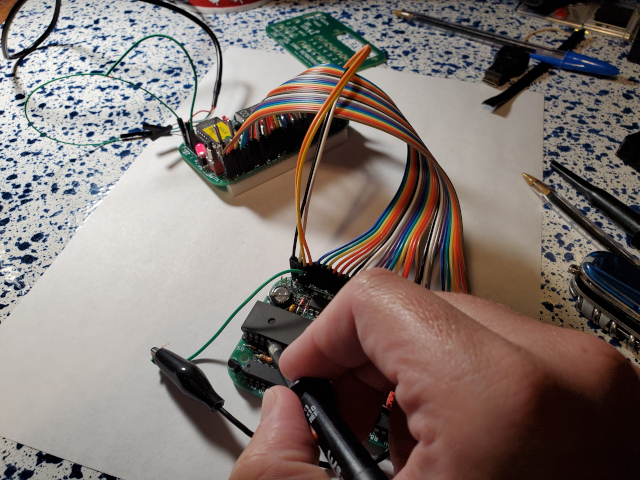
So the next thing I suspected was maybe the cards weren’t making good
connections with each other. I decided to connect the two halves
together using a ribbon of female to female jumper wires between the
headers, as shown in the picture above. I then set out to check the levels going into the CPU board
from the front panel. Everything was getting through to that point.
The switch states are all being communicated to the CPU board.
So I gave the CPU board a thorough once over next. I cleaned the flux
residue off, and then looked at the board connection by connection.
I found one solder bridge on two pins of the output latch. AHA!
I thought, perhaps this is just an output latching problem and the
bytes were getting into the RAM after all. I de-soldered these pins and
then re-soldered them, this time without a bridge. Now my front panel
only displays 00, and no LEDs come on.
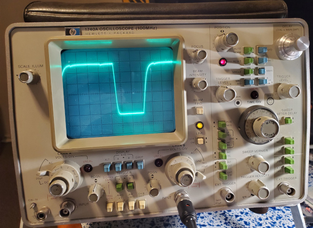
At this point, I decided it was time to break out my trusty HP 1740A
Oscilloscope and see what the CPU was doing when I put it into the
run state. (I am an analog scope snob, and also quite happy to be
using period-correct debugging tools on this project!) Touching the
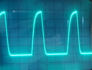
probe to bit 0 of the address line, we see
that the CPU is counting through its addresses! So then I wondered if
maybe it was working, but still having latch issues. I thought it best
to try to toggle in some program and see what happened. Lee Hart’s
manual has a couple of demo programs. One blinks the Q LED quickly, so
fast you can only see it change state by throwing the machine into the
wait state at the right moment. The other blinks slowly. I tried out
the first one, and it worked! Ten I toggled in the “Blink Q Slow”
program. The result can be seen below:
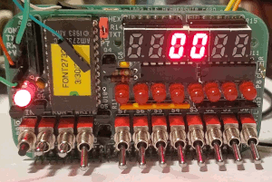
Success! I can toggle programs in and run them. I just can’t see the
output on the front panel. I have one blinking light, but I want all
those other lights to turn on, plus I want those segments all blinking
under my program control! So I decided I needed to check the inputs
going in to the output latch on the CPU board. Unfortunately, my logic
probe’s tip had gone missing. Oh well, the beast of an O-Scope from
the 1980s to the rescue once more!
The latch in question is a 74HC273 latch. It’s a fairly standard part,
consisting of 8 d-latches with a common clock and a tristate buffered
output enable. Basically it’s an 8-bit parallel register on a chip,
provided it is working correctly. I put the CPU into the wait state,
and then I touched the probe one at a time to the inputs of the
D latches. These are connected to the CPU’s data bus pins. The logic
levels were what I expected them to be! (I put in the pattern 101010
on the switches and then pressed “in”.) You can see in the animation
that I captured what the scope did as I went through each input. See,
an oscilloscope can be a rather nice, if somewhat expensive, logic
probe! I checked the output pins and….. they all stayed low all the
time.
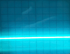
Ok, so the latch was getting good input for each bit, what about its
power levels for Vcc and Ground? They both checked out. No shorts
either. Then I took a look at the latch enable input while the CPU was
running a small program which keeps trying to send output out the pin.
As you can see below, the CPU was trying its hardest to latch the
output. The latch just wasn’t having any of it!
So then I decided to try out the monitor program. After all, if
I couldn’t have a nice front panel, maybe I could run via serial
terminal and play around a bit. I toggled in the jump to 0x8000,
started it up, and… nothing. A little bit of studying the schematic
made me realize that the 1802 has to latch the high order part of its
address in a separate 74HC273. I checked this latch, and it too was not
latching. Just like the output latch, it is receiving all correct
inputs; it just won’t open.
So that is where things are now. I can run programs that live entirely
in the lower 32k of RAM. The upper 32k isn’t accessible because of the
memory latch issue and the output port is also not latching. I’ll
continue to analyze and do point to point checks, but I am really
confused about what could be wrong now.
If you have some ideas, let me know in my
guestbook. Any ideas will be
appreciated! Once I fix it, I will post an update. So stay tuned!
UPDATE The debugging concludes in 1802 Membership Card Debugging – Part 2
 Computers
|
Home
|
Humor
|
Links Computers
|
Home
|
Humor
|
Links
|